How To Reduce PCB And Housing Mismatch In Smart Meter Component Sourcing
How To Reduce PCB And Housing Mismatch In Smart Meter Component Sourcing
In smart meter projects, PCB and housing mismatch is one of the most common causes of repeated sample changes, delayed approval, and unexpected OEM cost. A component may look correct in a drawing review and still become a problem later when the PCB, terminal structure, current path, mounting points, cover shape, and internal spacing are checked together in the real meter case. This guide explains how to reduce PCB and housing mismatch in smart meter component sourcing and how buyers and engineers can confirm structural fit earlier, before it slows down the whole project.
1. Why PCB And Housing Mismatch Happens So Easily
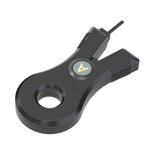
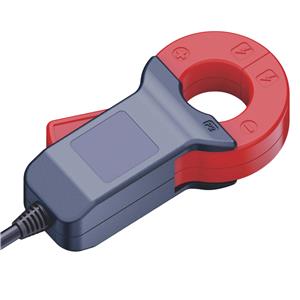
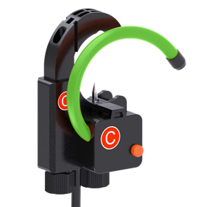
In many smart meter projects, component sourcing begins before the final internal structure is fully stabilized. At this stage, buyers may already be comparing current transformers, relays, shunt resistors, miniature voltage transformers, and meter cases. The problem is that each part may look acceptable on its own, but the project only becomes truly safe when all of them fit together inside the real housing and around the real PCB.
Mismatch often happens because teams confirm electrical function first and structural fit later. A current transformer may have the right ratio and still interfere with the enclosure height or terminal path. A relay may be suitable for switching duty and still create clearance problems with the cover or nearby parts. A meter case may look correct in external size but still fail to support the real PCB outline, screw positions, display opening, sealing structure, or terminal layout.
Another common reason is that the RFQ stage does not include enough structural information. If the supplier only receives a product name, current range, or general meter type, they may recommend a part that is close in category but not close enough in actual fit. This leads to the classic situation where the sample arrives, passes a basic technical check, and still cannot be used smoothly in the real assembly.
In short, PCB and housing mismatch is usually not caused by one bad part alone. It is caused by incomplete structural confirmation during sourcing and sample approval.
2. What Buyers And Engineers Should Confirm During Sourcing
The first thing to confirm is the PCB outline and key mounting positions. Buyers should make sure the supplier understands the board size, hole locations, connector or terminal areas, height limits, and any fixed keep-out zones. This matters because many component sourcing problems do not come from the part itself, but from how the part interacts with the actual board layout.
The second point is the internal housing structure. The case should not be treated as a separate item to be checked later. Buyers should confirm cover height, internal ribs, terminal block area, fixing points, display window position, sealing surfaces, and the real usable space inside the housing. What matters is not only the outer size of the case, but how much real internal freedom the design actually provides.
The third point is component direction and assembly sequence. A current transformer, relay, or miniature voltage transformer may technically fit in one orientation but still be difficult to assemble, solder, or protect after the housing is installed. Buyers should therefore confirm not only static dimensions, but also how the component will be mounted, how terminals or pins will align, and whether assembly remains stable in batch production.
The fourth point is tolerance and clearance margin. A layout that looks correct in theory may still become risky if there is not enough margin for molding variation, PCB tolerance, pin position variation, or housing deformation over time. In OEM projects, this is one of the most common hidden causes of repeated sample changes.
The fifth point is the relationship between technical approval and structural approval. A component should not be considered approved only because it meets electrical expectations. Buyers should confirm whether the same sample is also structurally safe for the housing, the real PCB, and the intended assembly process. This is especially important for CTs, relays, and meter cases.
Finally, buyers should check whether the supplier can support fit confirmation in a practical way. A stronger supplier should be able to review drawings, PCB layouts, internal structure photos, and dimensional notes instead of relying only on a general product recommendation.

| Check Area | Why It Matters | What Should Be Confirmed |
|---|---|---|
| PCB Outline And Holes | Defines whether the component can really be mounted correctly | Board size, hole positions, height limits, keep-out zones |
| Housing Internal Structure | Controls real usable space rather than external size only | Cover height, ribs, display window, sealing surfaces, terminal area |
| Component Direction | Affects assembly smoothness and structural safety | Mounting direction, pin alignment, terminal alignment, fixing logic |
| Tolerance And Clearance | Reduces hidden risk from variation in real production | Gap margin, molding tolerance, PCB variation, assembly allowance |
| Electrical + Structural Approval | Prevents approving a part that works electrically but fails physically | Real sample fit inside housing with the actual PCB and parts |
| Supplier Fit Support | Improves the chance of getting the right sample earlier | Drawing review, layout review, structural discussion, sample explanation |
3. How Buyers Can Reduce Mismatch Earlier
The most practical way is to send structural information early in the RFQ and sample stage. Buyers should provide PCB layout, internal housing drawings, key height limits, terminal structure, and any known assembly concerns together with the technical requirements. This allows the supplier to recommend parts that are closer to the final design instead of only category-correct.
It is also useful to treat fit confirmation as a separate milestone. A part may pass electrical review and still need additional structural confirmation before it is safe for the project. When buyers and engineers separate these two approval steps clearly, they usually reduce one of the most common hidden causes of sample delay and repeated revision.
Buyers should also check parts together, not only one by one. A current transformer, relay, shunt, or miniature voltage transformer may each fit individually, but the real question is whether they still fit together in the same housing with enough clearance and production tolerance. System-level review is what reveals this earlier.
Another useful principle is to compare suppliers by how well they support structural review. A lower-risk supplier usually provides more practical feedback on drawings, layout limits, mounting risk, and future batch consistency instead of only sending a standard sample quickly.
The best sourcing process is the one that finds PCB and housing mismatch before the project is already depending on an approved sample or fixed schedule.
Conclusion
Reducing PCB and housing mismatch in smart meter component sourcing requires more than checking electrical function or external dimensions alone. Buyers and engineers should confirm PCB outline, housing internal structure, component direction, tolerance margin, and real assembly fit before approving parts. When these points are reviewed together and early enough, the project becomes much less likely to face repeated samples, delayed approval, or costly structural rework later.
Contact Us
Looking for reliable smart meter components for your OEM project? Contact our team to discuss drawings, samples, technical requirements, and quotation details.